
Computational design and electrical characterization of printed electronic devices for empirical modeling techniques
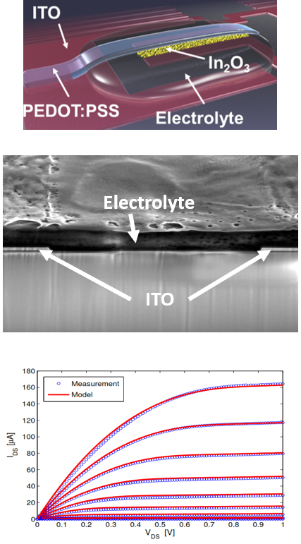
Solution processed and printed field-effect transistors can become very interesting for designing new applications on flexible and rigid substrates. However, a vast number of materials and fabrication routes exist to print such field-effect transistors. Since the state-of-the-art transistor models developed for silicon-based field-effect transistors do not capture the physics of these transistors, available transistor models are unfeasible to model printed transistors. Therefore, new models with the focus on printed materials needs to be developed to support circuit design for new applications. In this regard, empirical models are very interesting since they are data-driven and do not rely on the explicit description of the underlying transistor physics. For that reason, the aim in this subproject is to develop an empirical universal transistor model which can mimic the electrical characteristics of printed transistors even for various processes used in fabrication. Furthermore, interface properties between different material layers are studied including interface quality, thin film grain structures and geometry factors by high resolution microscopy techniques such as SEM and TEM. To that end suitable test structures arrays for the systematic evolution of electrical empirical models as well as test patterns for the study of ink/substrate interactions will be fabricated and characterized. Based on this experimental data, machine learning techniques will be employed to reduce the complexity of modeling parameter extraction.
| Name | Institute |
|---|---|
| Jasmin Aghassi | Institute of Nanotechnology (INT) |
| Gabriel Cadilha Marques | Institute of Nanotechnology (INT) |
| Xiaowei Feng | Institute of Nanotechnology (INT) |
| Name | Institute |
|---|---|
| Wolfgang Wenzel | Institute of Nanotechnology (INT) |
| Britta Nestler | Institute for Applied |